Für statistische Zwecke und um bestmögliche Funktionalität zu bieten, speichert diese Website Cookies auf Ihrem Gerät. Das Speichern von Cookies kann in den Browser-Einstellungen deaktiviert werden. Wenn Sie die Website weiter nutzen, stimmen Sie der Verwendung von Cookies zu.
Cookie akzeptieren
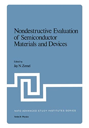
Nondestructive Evaluation of Semiconductor Materials and Devices
- Springer US
- 2013
- Taschenbuch
- 796 Seiten
- ISBN 9781475713541
From September 19-29, a NATO Advanced Study Institute on Non destructive Evaluation of Semiconductor Materials and Devices was held at the Villa Tuscolano in Frascati, Italy. A total of 80 attendees and lecturers participated in the program which covered many of the important topics in this field. The subject matter was divided to emphasize the following different types of problems: electrical measurements; acoustic measurements; scanning techniques; optical methods; backscatter methods; x-ray observations; accele rated life tests. It would be difficult to give a full discussion of such an Institute without going through the major points of each speaker. Clearly this is the proper task of the
Mehr
Weniger
zzgl. Versand
in Kürze